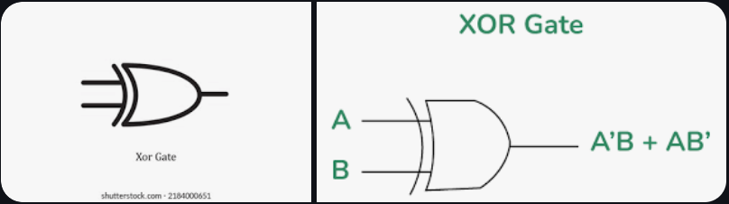
Exclusive-OR (XOR) Gate
- Output active-HIGH (=1) when exactly one input is HIGH.
- Only 2-input XOR gates exist; no 3- or 4-input versions.
- IEEE/ANSI symbol:
- Common ICs:
- 74LS86 (TTL)
- 74C86 (CMOS)
- 74HC86 (High-speed CMOS)
Exclusive-NOR (XNOR) Gate
- Output HIGH when inputs are equal (complement of XOR).
- Often implemented by connecting XOR output to an inverter.
- Common ICs:
- 74LS266 (TTL)
- 74C266 (CMOS)
- 74HC266 (High-speed CMOS)
Parity Generator and Checker
- Purpose: Detect single-bit errors in transmission by adding a parity bit.
- Even parity: total 1s (including parity bit) = even.
- Odd parity: total 1s (including parity bit) = odd.
Example 1: Even parity generator (4-bit data
Example 2: Odd parity generator (3-bit data
Combinational Circuits
- Output depends only on current inputs, no memory or feedback.
- Components: interconnection of logic gates transforming input data -> output data.
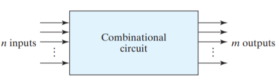
- Applications: Often connected to registers; if registers included -> sequential circuit.
- Standard combinational circuits:
- Adders
- Subtractors
- Comparators
- Decoders
- Encoders
- Multiplexers
Half-Adder (HA)
Purpose: Adds two single-bit inputs to produce sum and carry.
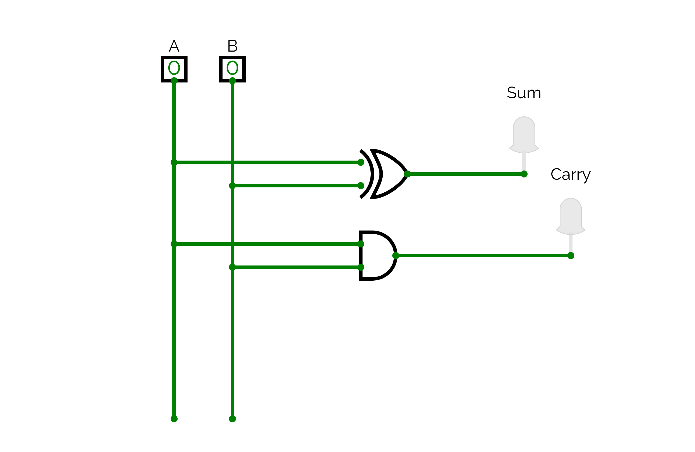
Inputs and Outputs
- Inputs:
, - Outputs:
- Sum (
) = - Carry (
) =
- Sum (
Truth Table
| A | B | Sum (S) | Carry (C) |
|---|---|---|---|
| 0 | 0 | 0 | 0 |
| 0 | 1 | 1 | 0 |
| 1 | 0 | 1 | 0 |
| 1 | 1 | 0 | 1 |
Logic Formulas
Explanation:
- Sum is HIGH when inputs are different.
- Carry is HIGH when both inputs are 1.
- Can only handle two inputs, so it cannot propagate carry from a previous addition.
Full-Adder (FA)
Purpose: Adds three single-bit inputs (including carry-in) to produce sum and carry-out.
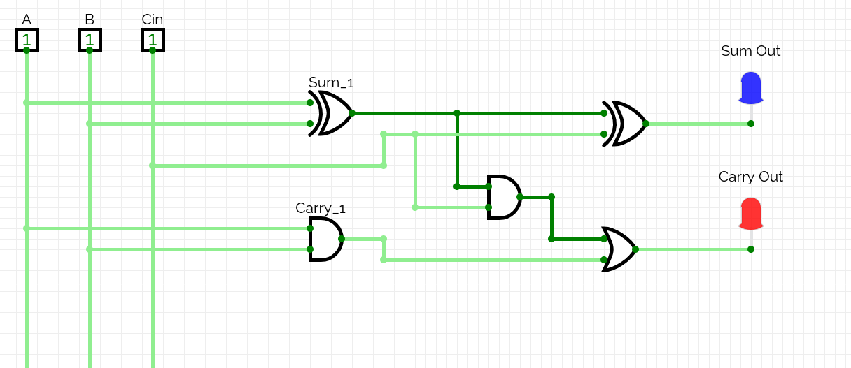
Inputs and Outputs
- Inputs:
, , - Outputs:
- Sum (
) = - Carry (
) =
- Sum (
Truth Table
| A | B | Cin | Sum (S) | Cout |
|---|---|---|---|---|
| 0 | 0 | 0 | 0 | 0 |
| 0 | 0 | 1 | 1 | 0 |
| 0 | 1 | 0 | 1 | 0 |
| 0 | 1 | 1 | 0 | 1 |
| 1 | 0 | 0 | 1 | 0 |
| 1 | 0 | 1 | 0 | 1 |
| 1 | 1 | 0 | 0 | 1 |
| 1 | 1 | 1 | 1 | 1 |
Logic Formulas
Explanation:
- Sum is HIGH when an odd number of inputs are 1.
- Carry-out is HIGH when at least two inputs are 1.
- Can handle carry from previous stage, so suitable for multi-bit addition.
Half-Subtractor (HS)
Purpose: Subtracts two single-bit inputs to produce difference and borrow.
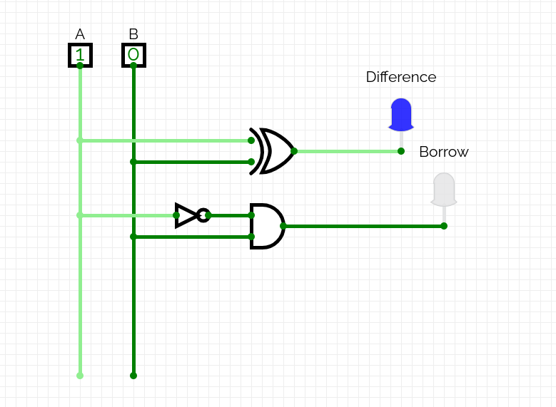
Inputs and Outputs
- Inputs:
, - Outputs:
- Difference (
) = - Borrow (
) =
- Difference (
Truth Table
| A | B | Difference (D) | Borrow (Bout) |
|---|---|---|---|
| 0 | 0 | 0 | 0 |
| 0 | 1 | 1 | 1 |
| 1 | 0 | 1 | 0 |
| 1 | 1 | 0 | 0 |
Logic Formulas
Explanation:
- Difference is HIGH when inputs are different.
- Borrow is HIGH when
and . - Cannot handle a borrow from a previous stage.
Full-Subtractor (FS)
Purpose: Subtracts three single-bit inputs (including borrow-in) to produce difference and borrow-out.
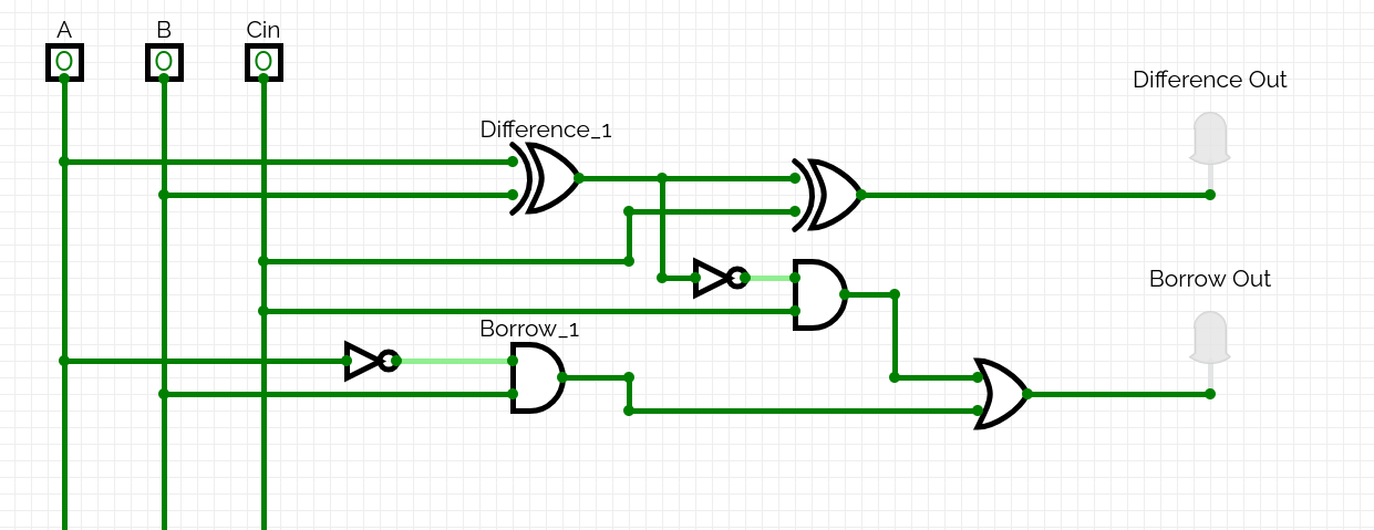
Inputs and Outputs
- Inputs:
, , - Outputs:
- Difference (
) = - Borrow (
) =
- Difference (
Truth Table
| A | B | Bin | Difference (D) | Bout |
|---|---|---|---|---|
| 0 | 0 | 0 | 0 | 0 |
| 0 | 0 | 1 | 1 | 1 |
| 0 | 1 | 0 | 1 | 1 |
| 0 | 1 | 1 | 0 | 1 |
| 1 | 0 | 0 | 1 | 0 |
| 1 | 0 | 1 | 0 | 0 |
| 1 | 1 | 0 | 0 | 0 |
| 1 | 1 | 1 | 1 | 1 |
Logic Formulas
Explanation:
- Difference is HIGH when an odd number of inputs are 1.
- Borrow-out is HIGH when subtraction requires borrowing.
- Can handle borrow from previous stage, making it suitable for multi-bit subtraction.
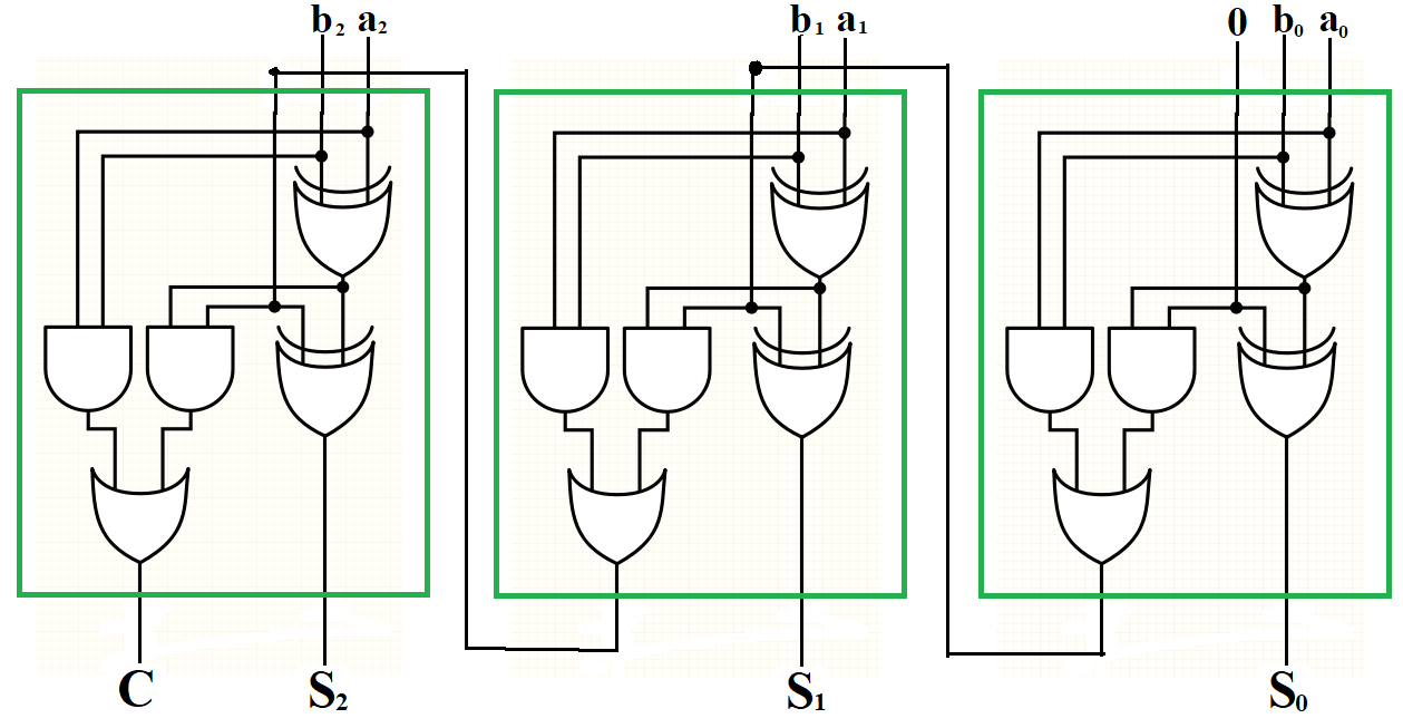
3-bit Adder
- Description: This is a 3-bit ripple carry adder composed of three Full Adder stages where the initial carry input is tied to 0 to perform binary addition.
- Logic Expression:
: Sum : Carry - Initial condition:
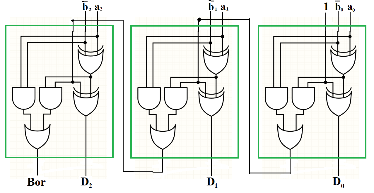
3-bit Subtractor
- Description: This circuit performs 3-bit binary subtraction (
) by feeding , the complement , and an initial borrow/carry of 1 into Full Adder stages to implement 2's complement logic. - Logic Expression:
: Difference : Borrow - Initial condition:
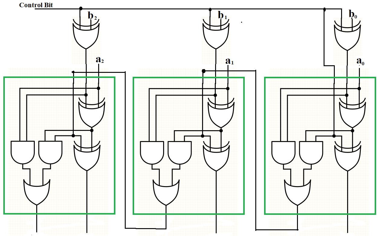
3-bit Adder-Subtractor
- Description: This multi-function circuit uses a Control Bit (
) and XOR gates to conditionally invert the inputs and set the initial carry, allowing it to act as either an adder ( ) or a subtractor ( ). - Logic Expression:
: Control Bit : Carry - Initial condition:
2's Complement Logic Circuit
Purpose: Represents negative numbers in binary and enables subtraction using addition.
Inputs and Outputs
- Inputs:
- Binary number:
- Control bit:
- Binary number:
- Outputs:
- 2's complement result:
- 2's complement result:
Logic Description
2's complement is generated in two steps:
- One's complement: invert all bits
- Add 1 to the inverted result
Logic Formulas (per bit)
1-Bit Truth Table (with Carry-In)
| A | Cin | Sum | Cout | |
|---|---|---|---|---|
| 0 | 0 | 1 | 1 | 0 |
| 0 | 1 | 1 | 0 | 1 |
| 1 | 0 | 0 | 0 | 0 |
| 1 | 1 | 0 | 1 | 0 |
Explanation
- Bitwise NOT converts
to one's complement - Adding 1 completes the 2's complement
- Enables subtraction using:
- Used internally in ALUs and CPUs
Arithmetic and Logic Unit (ALU)
Purpose: Performs arithmetic and logical operations on binary data.
Inputs and Outputs
- Inputs:
- Operands:
, - Control signals:
,
- Operands:
- Outputs:
- Result:
- Status flags (optional): Zero, Carry, Overflow
- Result:
Example Operation Selection Table
| S1 | S0 | Operation | Description |
|---|---|---|---|
| 0 | 0 | Addition | |
| 0 | 1 | Subtraction (2's comp) | |
| 1 | 0 | AND | |
| 1 | 1 | XOR |
Internal Logic
- Arithmetic block
- Full adders
- 2's complement logic for subtraction
- Logic block
- AND, OR, XOR, NOT gates
- Multiplexer
- Selects output based on control signals
Explanation
- ALU is the core computation unit of the CPU
- Uses control signals to choose the operation
- Combines adders, logic gates, and multiplexers
- Scales to multi-bit designs (e.g., 32-bit, 64-bit)
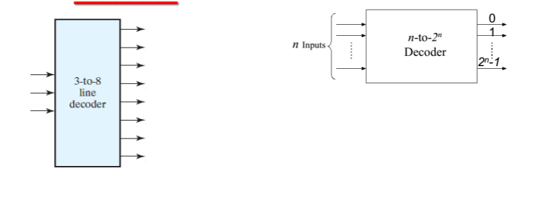
Decoder
- Function: A decoder activates exactly one of its
output lines based on the binary combination of its input lines. - Complexity: An
-to- decoder requires AND gates, each with inputs.
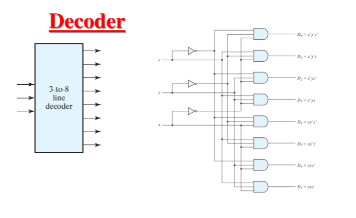
Logic Implementation of a 3-to-8 Decoder
For a 3-to-8 decoder with inputs
(Binary 000) (Binary 001) (Binary 010) (Binary 011) (Binary 100) (Binary 101) (Binary 110) (Binary 111)
Formulas for Decoder Logic
Since you are working with LaTeX in Markdown, here is how you would formally represent the output logic for a specific line (e.g.,
Or using the "prime" notation seen in your image:
Design a 2-bit multiplier using decoder
The table below shows the relationship between two 2-bit inputs (
Mathematically, this represents
| 0 | 0 | 0 | 0 | 0 | 0 | 0 | 0 |
| 0 | 0 | 0 | 1 | 0 | 0 | 0 | 0 |
| 0 | 0 | 1 | 0 | 0 | 0 | 0 | 0 |
| 0 | 0 | 1 | 1 | 0 | 0 | 0 | 0 |
| 0 | 1 | 0 | 0 | 0 | 0 | 0 | 0 |
| 0 | 1 | 0 | 1 | 0 | 0 | 0 | 1 |
| 0 | 1 | 1 | 0 | 0 | 0 | 1 | 0 |
| 0 | 1 | 1 | 1 | 0 | 0 | 1 | 1 |
| 1 | 0 | 0 | 0 | 0 | 0 | 0 | 0 |
| 1 | 0 | 0 | 1 | 0 | 0 | 1 | 0 |
| 1 | 0 | 1 | 0 | 0 | 1 | 0 | 0 |
| 1 | 0 | 1 | 1 | 0 | 1 | 1 | 0 |
| 1 | 1 | 0 | 0 | 0 | 0 | 0 | 0 |
| 1 | 1 | 0 | 1 | 0 | 0 | 1 | 1 |
| 1 | 1 | 1 | 0 | 0 | 1 | 1 | 0 |
| 1 | 1 | 1 | 1 | 1 | 0 | 0 | 1 |
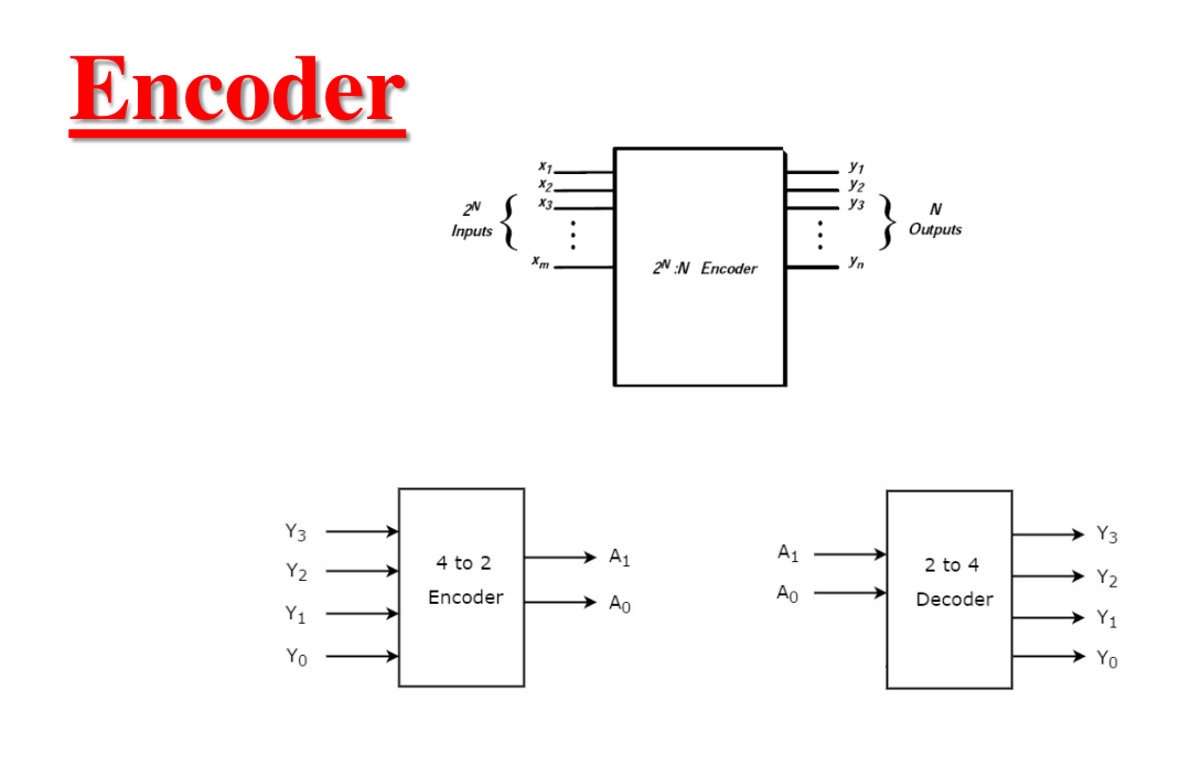
Encoder
Truth Table of an Octal-to-Binary Encoder
The following table represents the logic of an 8x3 encoder, where each of the eight input lines (
| 1 | 0 | 0 | 0 | 0 | 0 | 0 | 0 | 0 | 0 | 0 |
| 0 | 1 | 0 | 0 | 0 | 0 | 0 | 0 | 0 | 0 | 1 |
| 0 | 0 | 1 | 0 | 0 | 0 | 0 | 0 | 0 | 1 | 0 |
| 0 | 0 | 0 | 1 | 0 | 0 | 0 | 0 | 0 | 1 | 1 |
| 0 | 0 | 0 | 0 | 1 | 0 | 0 | 0 | 1 | 0 | 0 |
| 0 | 0 | 0 | 0 | 0 | 1 | 0 | 0 | 1 | 0 | 1 |
| 0 | 0 | 0 | 0 | 0 | 0 | 1 | 0 | 1 | 1 | 0 |
| 0 | 0 | 0 | 0 | 0 | 0 | 0 | 1 | 1 | 1 | 1 |
Logic Equations
Based on the truth table, the Boolean expressions for the outputs are derived by identifying which input lines activate each specific output bit:
Priority Encoder
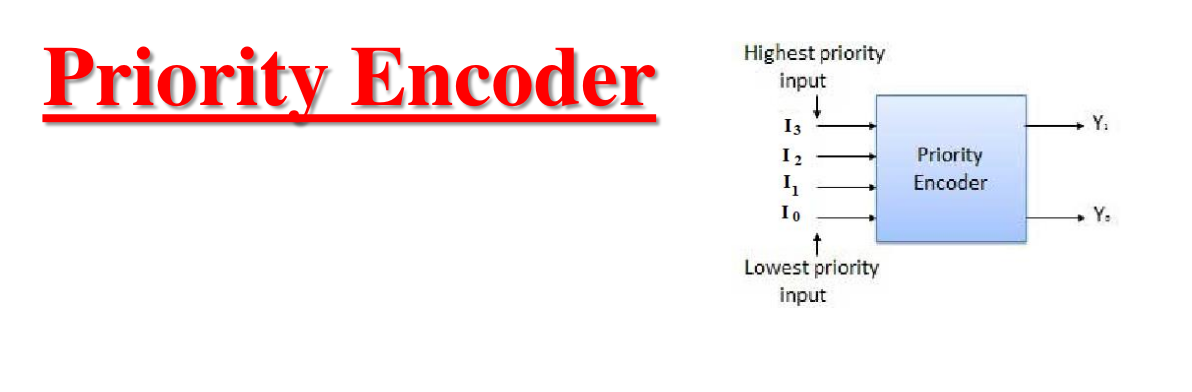
Understanding Priority Encoders
In a standard encoder, only one input can be active at a time. A priority encoder solves this limitation by ensuring that if two or more inputs are high simultaneously, the input with the highest priority takes precedence.
For the 4-bit priority encoder shown:
- If
is 1, the output will be 11regardless of the states ofand . - If
is 0 and is 1, the output will be 10regardless ofand .
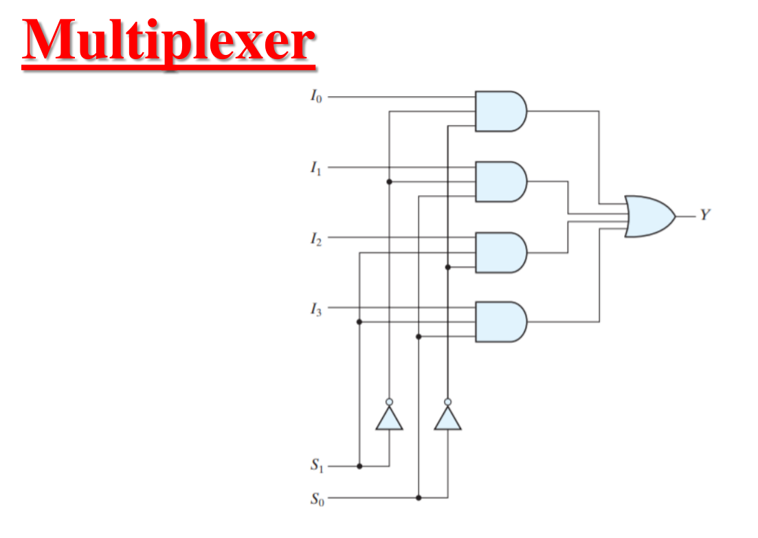
Multiplexer
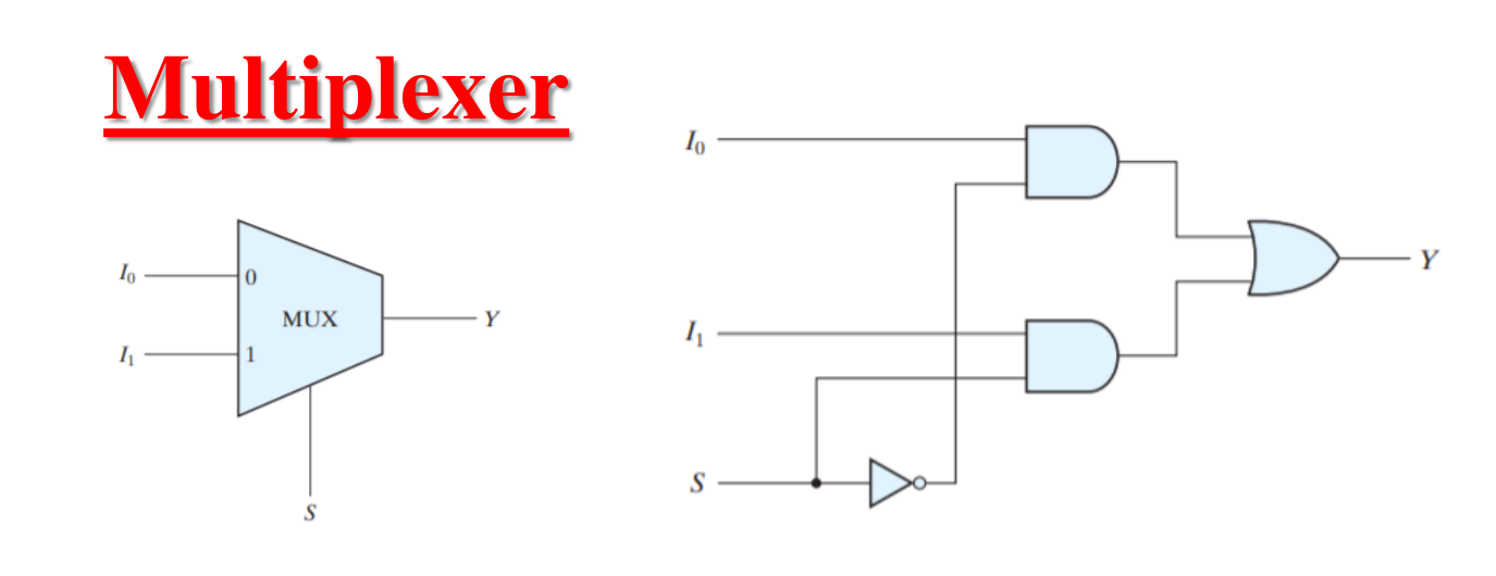
Truth Table: 2-to-1 Multiplexer
For a 2-to-1 MUX, the select line
| S | Y |
|---|---|
| 0 | |
| 1 |
Boolean Equation:
Truth Table: 4-to-1 Multiplexer
For a 4-to-1 MUX, two select lines (
| S1 | S0 | Y |
|---|---|---|
| 0 | 0 | |
| 0 | 1 | |
| 1 | 0 | |
| 1 | 1 |
Boolean Equation: